← Accueil actu | Salle du marché
2026-09-11 · Source:TechRadar
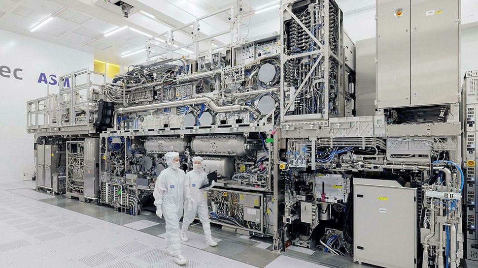
Intel claims cumulative High-NA EUV output has crossed the one-million-wafer mark, accounting for roughly three out of every four such wafers ever exposed anywhere in the industry.
Intel says its cumulative output of High-NA EUV wafers has crossed the one-million mark, a volume the company claims is larger than that of the rest of the semiconductor industry combined. According to the figures cited by TechRadar, roughly three-quarters of every High-NA wafer ever exposed has run through Intel's production lines, making the chipmaker by far the heaviest user of the next-generation lithography technology to date.
High-NA EUV represents the leading edge of lithography development, and wafer volume on such tools is widely watched as a proxy for how far a manufacturer has moved the technology from engineering evaluation toward volume manufacturing. By Intel's own accounting, its exposure count has no peer: the remaining quarter of all High-NA wafers ever processed is shared among every other chipmaker in the industry.
For a company racing to re-establish process leadership, the milestone carries weight beyond the headline number. Accumulating a million wafers on a new patterning platform implies an extensive base of process learning — overlay control, defectivity management, yield tuning — that typically cannot be replicated quickly by competitors who have exposed far fewer wafers. Volume, in lithography terms, is a compounding asset: each run contributes data that shortens the path to mature, cost-effective production.
The claim also feeds directly into Intel's manufacturing credibility. Demonstrated High-NA volume signals to customers and investors that the company's process roadmap is being exercised at scale rather than in laboratory quantities. The figures are self-reported, however, and the source does not break the total down by product, tool count or timeframe. Even so, if the numbers hold, the bulk of hands-on experience with the industry's most advanced patterning technology currently sits inside Intel's own fabs — an advantage that could prove difficult for rivals to close quickly.
Mots-clés: Intel · High-NA EUV · EUV Lithography · Semiconductor Manufacturing · Wafer Production
萬安算交所 AIXX · AIXX · Bourse compute vérifiée · Accéder à la salle